The charge density distribution, which fully defines the ground-state properties of a material system, can be accurately measured in single crystals using X-ray diffraction. However, there is still a lack of experimental techniques capable of measuring charge density redistribution in defective or heterogeneous crystals at the relevant atomic scale with the required precision. While this information can be effectively evaluated by modern numerical methods such as DFT, these theoretical predictions still require experimental validations. Four-dimensional scanning transmission electron microscopy (4D-STEM) is a modern technique in which a full diffraction pattern is recorded at each electron probe position. While it offers a powerful means to simultaneously resolve atomic structure and probe local electric fields and charge densities, accurate quantification at the atomic scale remains challenging due to probe propagation, size and aberration-related effects. As a consequence of it, charge redistribution phenomena have only been discussed qualitatively by 4D-STEM.
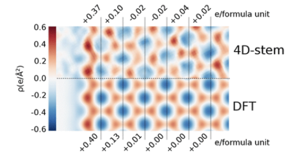
In a recent work, we used 4D-STEM to analyze electric fields and charge densities in both pristine and defective h-BN monolayers, combining experimental results with first-principles simulations. This work presents precise measurements of positive charge accumulation at an h-BN monolayer free edge, showing excellent agreement with DFT predictions. This demonstrated that 4D-STEM can reliably detect charge transfer phenomena at the single unit cell scale with sensitivity down to a few tenths of an electron.
This work appeared in ACS nano
L. Susana, A. Gloter, M. Tencé and A. Zobelli, Direct quantifying charge transfer by 4D-STEM: a study on perfect and defective hexagonal boron nitride, ACS Nano 18, 7424 (2024)