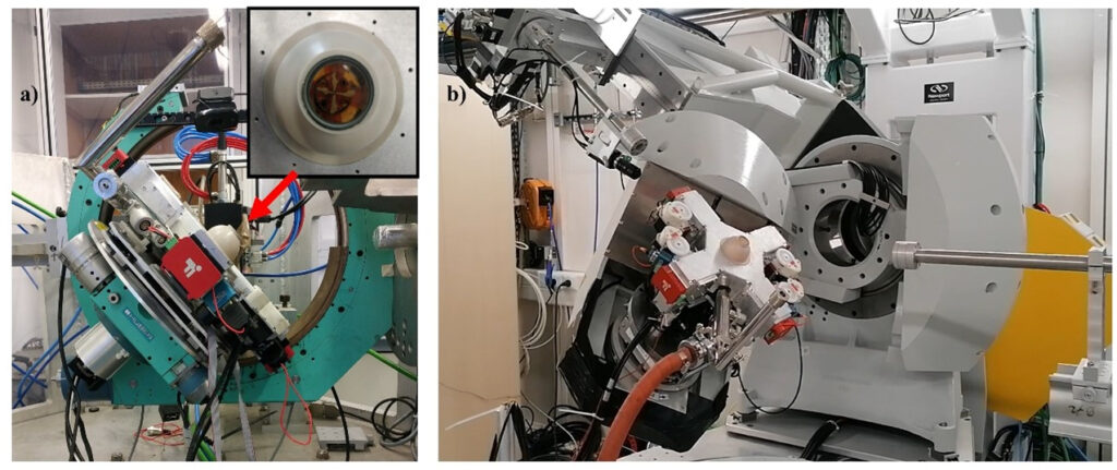
Researchers and engineers at the Solid State Physics Laboratory (LPS) (UMR of the CNRS and the University of Paris-Saclay) have developed an innovative device capable of applying biaxial mechanical deformations to two-dimensional materials at cryogenic temperatures. This was done by in-situ probing of the 3D deformation of the atomic lattice by X-ray diffraction (XRD) as well as the electronic properties. Thanks to this device, they were able to demonstrate a novel behavior of correlated electrons that align in the direction of mechanical traction, a behavior that is directly correlated to the modification of the system’s symmetry. They were also able to show that the transition temperature to this state varies by an impressive 30 K, which opens up new perspectives on the manipulation of electronic states in 2D systems by mechanical deformation.
2D materials have attracted a lot of attention from the scientific community because of their unique electronic properties related to low dimensionality effects. Unlike three-dimensional materials, they allow flexible control of their properties by mechanical, electronic, optical and magnetic excitations. Their lamellar structure, composed of weakly bound atomic planes, generates anisotropic properties, influencing in particular electronic conduction. Some are superconductors, others semiconductors or optoelectronics, opening the way to applications in electronics and photovoltaics. However, the link between the microscopic organization of matter and electronic properties is not always well understood, but represents a definite challenge for the control of electronic properties by modification of atomic structure. To address this issue, researchers and engineers at the LPS have developed a unique biaxial tensile device capable of applying mechanical deformation to 2D compounds over a wide temperature range (15-400 K). This device is designed to be compatible with measurements that monitor structural deformations (by DRX) and electronic properties (by transport measurements) during deformation.
To highlight the link between atomic structure and electronic properties, LPS researchers, in collaboration with the Pprime Institute in Poitiers and the Néel Institute in Grenoble, have been studying a 2D material, TbTe3, with particularly remarkable intrinsic properties.
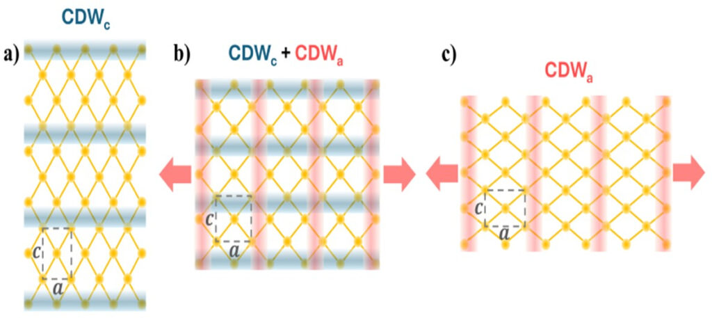
The ground state of this system is composed of a stack of 2D planes weakly bound together in the direction of the stack (Van der Waals type bonds) which have an almost (but not!) square structure in the planes, with a relative deviation of only 0.2% between the a and c lattice parametersof the square – with c > a. However, from the point of view of electronic properties, the electrons behave very differently depending on the main directions in the plane. At room temperature, the electron density is spatially modulated in the c direction, in which the atoms are most widely spaced, but not in the perpendicular a direction (Fig. 2a). This modulated phase is called a Charge Density Wave (CDW). Thanks to the biaxial tensile device developed, the consortium’s researchers were able to alter the atomic structure in the planes, first giving it a square geometry (a=c) (Fig. 2b) by applying an elongation along a, then rectangular with an inversion of the anisotropy direction (a>c) (Fig. 2c). By combining XRD and electron transport measurements, they observed that the ODC modulation changed orientation and gradually appeared in the tensile direction, with the two coexisting when a = c. They thus demonstrated that the symmetry of the atomic structure in the planes has a direct impact on the symmetry of the electronic properties.
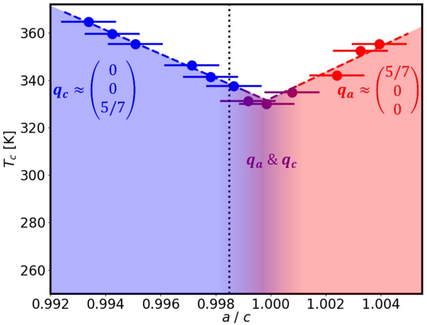
Furthermore, they were able to observe that the temperature at which the CDW appears varies by more than 30 K under mechanical deformation, while the amplitude of the CDW formed under traction remains perfectly stable. This discovery calls into question current theoretical models of CDW, particularly the Peierls model. This significant increase in the transition temperature opens up very promising prospects for the study of other electronic phases in 2D systems, particularly superconductivity. In addition, CDW sliding experiments have been able to show the incommensurability of this new traction-induced CDW with the host atomic lattice. This collective conduction mode, which is still poorly understood, originates in the spatial and temporal fluctuations of the electronic modulation phase. These measurements have enabled the establishment of a phase diagram of TbTe3 under tension in the temperature range 250 K – 380 K (Fig. 3).
This innovative methodology represents a significant step forward in the exploration of electronic order phenomena that coexist or compete within condensed matter. By enabling the precise manipulation of atomic structure and the modulation of electronic properties at the microscopic scale, it offers a new perspective for probing the mechanisms underlying these complex phenomena. This promising approach thus opens up new prospects for the fundamental understanding of the physics of materials and for the development of innovative electronic and quantum devices.
Part of this research has been published in the scientific journal “Nature Communications”.
Nature Communications, volume 15, Article number: 3667 (2024)